Custom Ceramic Substrates & Thermal Plates
Direct-factory manufacturing of precision ceramic substrates in Alumina (Al₂O₃), Aluminum Nitride (AlN), and Beryllium Oxide (BeO). Supporting DBC, AMB, and bare substrate formats for power electronics, semiconductor packaging, and thermal management systems.
Substrate Capabilities
Dimensional tolerance to ±0.003 mm, surface flatness <5 μm per 25 mm, and Ra 0.02 μm finish. Metallization options include thick film printing, thin film deposition, and direct copper bonding. All substrates inspected per drawing specification with full dimensional reports.
Available Substrate Materials
Select the optimal ceramic material for your thermal and electrical requirements
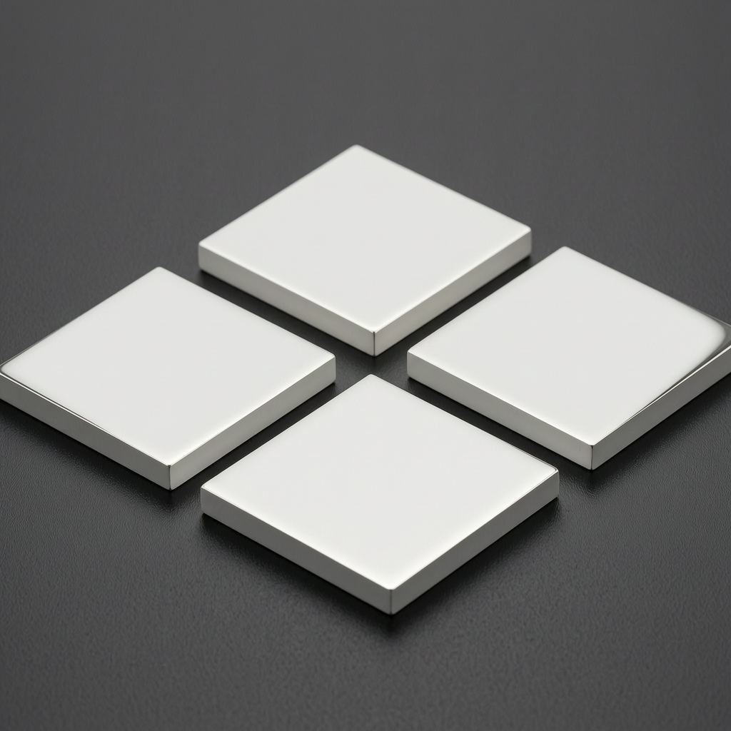
Alumina (Al₂O₃)
Grade: 96%, 99.5%, 99.8%
Standard substrate for thick/thin film circuits and power modules
Aluminum Nitride (AlN)
Grade: High purity
High-performance thermal management for power electronics and LED packaging
Beryllium Oxide (BeO)
Grade: Technical grade
Exceptional thermal conductivity for aerospace and RF applications
Substrate Formats & Configurations
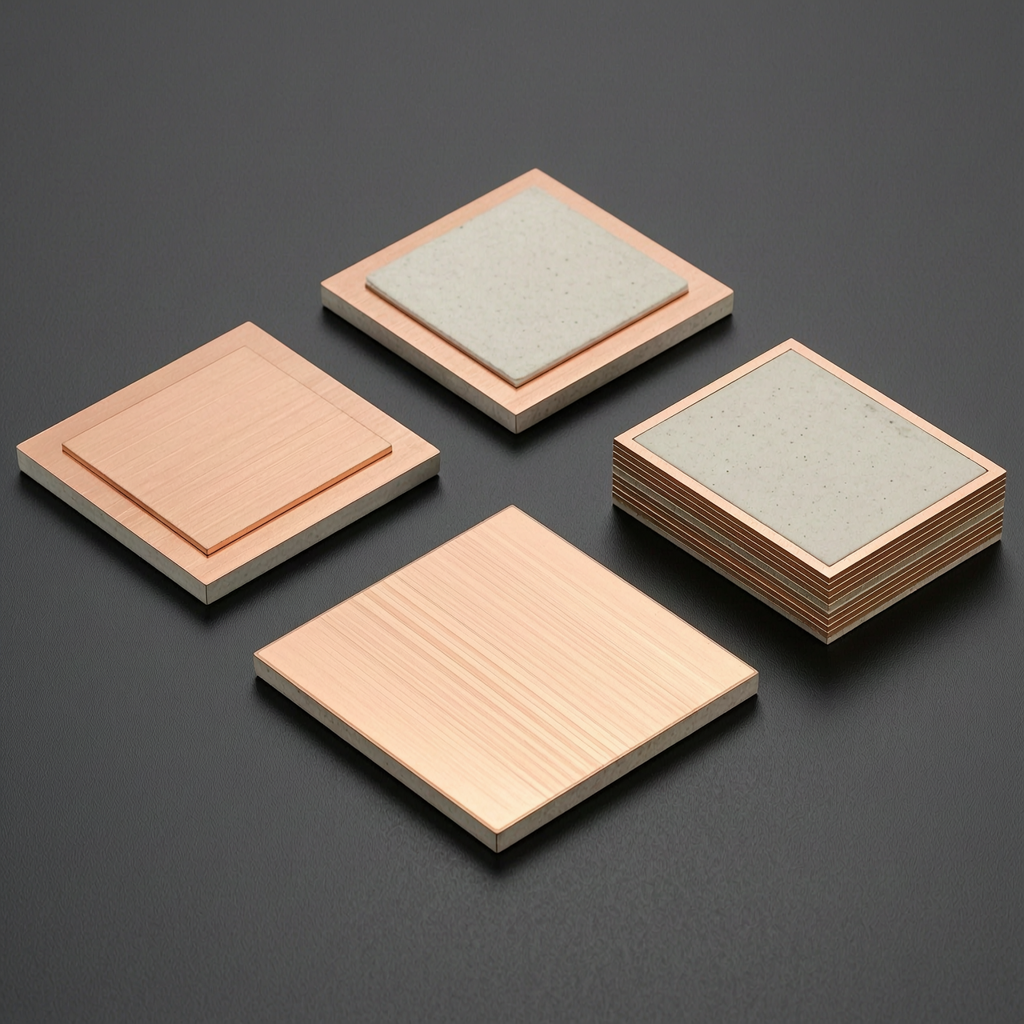
Direct Bonded Copper (DBC) Substrates
Al₂O₃ and AlN substrates with bonded copper layers for power module assemblies
Active Metal Brazed (AMB) Substrates
Si₃N₄ ceramic substrates with active brazed copper for high-reliability power applications
LTCC / HTCC Substrates
Multi-layer co-fired ceramic substrates with embedded conductors and vias
Bare Ceramic Plates
Flat polished substrates in custom dimensions for hybrid ICs and sensor platforms
Precision Capabilities
Actual achievable tolerances depend on material, geometry, feature dimensions, and drawing requirements.
Target Applications
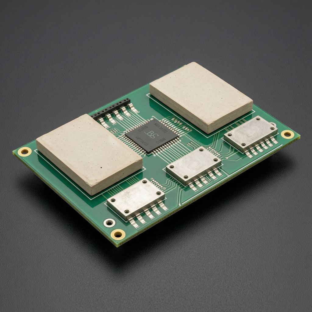
Power Electronics
- -IGBT module substrates
- -MOSFET thermal pads
- -Gate driver boards
- -Bus bar insulators
Semiconductor Packaging
- -LED heat spreaders
- -Laser diode submounts
- -RF/microwave packages
- -MEMS sensor platforms
Thermal Management
- -Heatsink insulators
- -Thermal interface plates
- -Phase-change material carriers
- -Cold plate substrates
What Are Ceramic Substrates Used For?
Ceramic substrates serve as the foundational platform for electronic circuits, power modules, and thermal management systems. Manufactured from alumina, aluminum nitride, and beryllium oxide, these substrates provide electrical insulation while enabling efficient heat transfer. Available as bare ceramic plates, Direct Bonded Copper (DBC), Active Metal Brazed (AMB), and LTCC/HTCC multi-layer configurations, substrates are used in IGBT modules, LED packaging, RF/microwave circuits, and power electronics. Precision machining achieves tight dimensional tolerances, flatness requirements, and surface finishes suitable for metallization and thin/thick film circuit processing.
Critical Features of Ceramic Substrates
| Feature | Engineering Significance | Inspection Method |
|---|---|---|
| Thickness | Thermal resistance, mechanical strength | Micrometer / CMM |
| Flatness | Metallization adhesion, circuit planarity | Optical flat / laser interferometry |
| Parallelism | Uniform thickness, stacking | Surface plate / height gauge |
| Surface Finish | Thin/thick film adhesion, metallization | Roughness tester (profilometry) |
| Hole Position | Via alignment, mounting accuracy | Video measuring system |
| Slot Dimensions | Component fit, circuit isolation | Video measuring system |
| Linear Dimensions | Overall size, mounting pattern | CMM |
Capability Context
The following capabilities represent demonstrated manufacturing results. Final achievable tolerances depend on material grade, substrate size, and specific requirements.
| Feature | Representative Capability | Applicable Context | Inspection |
|---|---|---|---|
| Dimensional Tolerance | ±0.003 mm | Standard substrate sizes | CMM |
| Surface Flatness | <5 μm per 25 mm | Lapped substrates | Optical flat / laser interferometry |
| Surface Finish | Ra 0.02 μm | Polished for metallization | Roughness tester |
| Minimum Trace Width | 50 μm | Thick/thin film circuits | Video measuring |
| Via Hole Diameter | ≥0.15 mm | Metallized vias | Video measuring |
| Thickness Range | 0.25 - 2.0 mm | Standard substrate range | Micrometer |
Capabilities shown represent demonstrated or achievable manufacturing results. Final tolerances depend on ceramic material, part size, geometry, feature location, surface requirements and inspection method. Requirements are confirmed during drawing review.
Manufacturing Process for Ceramic Substrates
Surface Grinding
Precision surface grinding to achieve thickness tolerance and initial flatness. Applicable to all substrate materials.
Lapping
Precision lapping for flatness <5 μm per 25 mm and Ra 0.02 μm surface finish. Critical for metallization.
Polishing
Mirror polishing for thin-film circuits and optical applications. Confirmed for AlN and Al₂O₃ substrates.
Metallization
Thick film and thin film metallization for circuit patterns. Confirmed for AlN and Alumina substrates.
DBC Bonding
Direct Bonded Copper process for AlN and Al₂O₃ substrates. Up to 200x200 mm capability.
Via Drilling & Patterning
Precision via hole drilling and slot machining for circuit interconnection. ≥0.15 mm via capability.
What to Include in Your Substrate Drawing or RFQ
Dimensions & Thickness
Length, width, thickness with tolerances. Include flatness and parallelism requirements for critical surfaces.
Material & Metallization
Ceramic type (Al₂O₃, AlN, BeO), grade, and metallization requirements (DBC, thick film, thin film).
Surface Finish Requirements
Ra values for metallization surfaces. Standard polished: Ra 0.02 μm. Specify which surfaces require finish.
Hole Pattern & Quantity
Via hole diameter, position, quantity. Include circuit pattern files if applicable. Prototype or production quantity.
Related Engineering Resources
All Ceramic Components
Explore our full range of precision ceramic components
Material Selection Guide
Compare substrate materials for electronic applications
Power Electronics Applications
Explore substrate requirements for power modules
Quality & Inspection
Flatness, surface finish, and dimensional capabilities
Submit Your Substrate Drawing for Review
Upload your 2D blueprints or 3D CAD files (.STEP / .IGS). Our engineering team will perform a DFM review and provide a competitive quote within 24 hours. Prototype substrates available within 7-10 business days.
Submit Drawing for 24-Hour Review